maanantai 18. joulukuuta 2023

Project update 2023

So, last post seems to be from summer 2021. Not even that long ago, eh? :D Well, time for an update then!

Anyhoo, paradoxically a lot has happened regarding the project, and also, not so much. Summarizing:

  1. Laser-cut plywood prototype case
  2. KAPE GPU PCB version
  3. Address Decoder design
  4. Plan for the CPU board
  5. Plan for the keyboard

Laser-cut Plywood Prototype Case 

Early this summer I had the possibility to use a laser cutter. I of course opted out to use it to print a new prototype case for KAPE. I now finally managed to assemble it! Pictures tell more than a thousand words, so have over 5000 words:


I was thinking of finishing the plywood with some wax oil - it might make the wood pop visually more, and also would give it a protective coating. I'd have to try the one I'm thinking of using on a scrap piece of that same plywood to make sure it looks good and doesn't ruin anything. 

The backplate also doesn't have all the necessary outputs yet. There's only a reset button and a power switch, as well as a hole for SCART. The access to the laser cutter was very time-limited, so I had to rush the design a bit. If not for that forced rushing, I'd have designed a changeable backplate. 

The top cover can be lifted, and is secured with screws on the side. I made them sunk by adding a plywood spacer in the holes. With more time I'd've thought of a better position for the screws, as it's quite annoying that the screws are on the side. But at least this way you don't have to flip the computer to get to the screws, or the screws being ugly and visible at the top.

Also, the current breadboard version, and possibly not even the minimized breadboard version, won't fit in the case, but the PCB version should fit nicely. I haven't even designed it yet so this is just wild guesswork.

KAPE GPU PCB Version

KAPE GPU has been transferred to a PCB version - however there were some bugs. I forgot one important resistor between +5V and SCART select source signal, so that the mode is changed from composite to RGB.


The board isn't fully populated yet - I soldered just enough parts to test that the AL422B I bought specifically for this board works properly... ...and it didn't. It ALMOST works - everything else works fine except D0 out. This could also mean D0 in could actually be the one that is broken. OR the chip's bit 0 circuit is fried. 

I tried to bughunt in case it was something wrong with my routing or maybe I have a short somewhere or some other design blunder that makes it not work properly, so I tried stuff like cutting a specific ground line and jumpering from another side, etc. but it just looks like the chip is borked. Either I broke it, or it was broken when I got it. 

I will be doing a thorough re-test, and if I can't figure it out, I'll try to desolder and replace the AL422B chip with another one I have on hand. If I'm not able to desolder it, I'll just populate a new board - I still have some spares left.

Address Decoder Design

I recently mulled about the Address Decoder. I have been thinking about external buses and peripheral cards and auto-config or manual config etc., but I decided I was thinking too complex, at least for now. So I revisited the Address Decoder, and it's still maybe a bit too complex, but it's a lot more simple than what I was thinking earlier. 


I mean, sure, it looks a lot more complex than the one I presented in an earlier post, but that only had RAM, RAM and ROM, or RAM, ROM, and GPU in it. I talked about having a comparator for each device to select it, but that would result in one comparator per device PLUS all the needed glue logic. This way, I can get 8 devices with only 6 chips. With a PLD that count goes to 2, if you want to keep the device memory tightened to a single 256-byte page, or just the PLD if we forgo that and reserve 2K for device memory mapping.

This is the resulting memory map from this address decoder design. Oh and I have already started breadboarding it!


Plan for the CPU Board

Currently the CPU board (as of now, still in breadboards) looks like this:


I have circled red everything that will be (eventually) going the way of the dodo. In essence, my plan is to strip all debugging and uploading, remove the overtly complex clock design, and remove the old address decoder. I will be adding a ROM and at least the UM6551 for serial communication, a single clock source for 2 MHz, and the new address decoder. With any luck, it will only take 4-5 breadboards and fits in a lot smaller footprint. I might even be able to fit it in the new prototype case even if they were still on breadboards!

First tho, I will be fixing the current wirings, for helping with programming the ROM and UM6551, which I will be adding to it once I'm sure everything works correctly. I'll also probably get rid of the old address decoder and old clock at this point and replace them with the new ones. Once everything is working, I'll get rid of the debugging systems and minimalize the whole thing. At this point I'll hopefully have also figured out how to program an ATF22V10C (or GAL22V10) chip, so I can get rid of most of the address decoding chips.

After that, it's just adding the 6552, SD card interface and YM2149F, figure out the outputs and cabling and power, and we're as good as done! 

Plan for the Keyboard

The keyboard has 61 keys, and the plan is to have the the keyboard controller send the scancode as a 6-bit value, and also as ASCII every other byte. Using 7-bit ASCII, we get the top-bit be an identifier bit in case the CPU side gets somehow out of sync. The unused bit in the scancode could then be used for state change info. The data is presented to the CPU only if there is an event, otherwise reading the keyboard controller results in a 0.

8bit keyboard read data
00000000               No event. Read again, if another zero,
                       no key events since last full read.

0ESSSSSS
||     |
||     \-- bits 0 - 5: SSSSSS - 6bit ScanCode
|\-------- bit 6:      E - 1bit Event, 0 -> key released, 1 -> key pressed. 
                       If key pressed, next byte is and ASCII of this scancode
\--------- bit 7:      0 -> Scancode 1 -> ASCII 

1AAAAAAA
|      |
|      \-- bits 0 - 6: AAAAAAA - 7bit ASCII
\--------- bit 7:      0 -> Scancode 1 -> ASCII 


The keyboard matrix scan will be processed 1 kHz fullscan, with a 15x5 keyboard matrix. When a key is processed it's state is detected with the matrix scan, and compared to a previous state. In case the state has changed, the scan code is enqueued in a queue-buffer. If the state was pressed, the scan-code is translated to ASCII, bit 7 is set, and that also is enqueued. 

I will use the ATmega16A for the keyboard controller, as it has more than enough pins to do a 15x5 matrix, and some control signals. It will be too slow to interact with the databus with interrupts, but with a little help from our friend, the 74HC573 tri-state latchable register, we can use the address decoders Keyboard Read -signal as the OE for the register, and also as an interrupt to let the Keyboard Controller know that a value has been read. 

Even if the ATmega16A isn't fast enough to respond directly to a databus, it's more than fast enough to read a value from the queue buffer and output it to a register. If my calculations are correct, 6502 takes 4 cycles to LDA absolute address, and I will be running the 6502 at 2 MHz. That means the keyboard controller has 8 cycles per a 6502 cycle. If not with C, hacking with some assembly I'm sure I can make it work. 

When in the interrupt, we'll dequeue the next scancode/ASCII from the queue-buffer, and latch it to the register chip. In case we don't have anything to dequeue, we'll latch 0. This lets the CPU know that now keyboard events have happened. Since reading the register is the only way to update it, the 6502 might need to read 0 twice to make sure we don't miss any keyboard input in a frame.


Summa summarum

So, been awhile. 

Not much has happened, but there's definite progress anyway. Baby steps but steps anyway. Once I get (in the next 12 months, I bet) the GPU (both breadboard version and PCB version are currently "offline") fixed, the ROM installed, and the UM6551 serial connection for program upload done, I can start to figure out things like 6522, SD card interface, keyboard, YM2149F, gamepads/joysticks, etc.

Still haven't decided whether I'm gonna use NES pads, SNES pads or regular C64/Amiga -style joysticks, but there's plenty of time to figure it out.

Here's hoping I'll make the next blog update a bit earlier than in 30 months next time!

perjantai 7. toukokuuta 2021

KAPE MB (mainboard) finally taking shape!

It's a been a hot few months since the last blog update. For my defense, nothing really major has happened with the project, even though I've been working on it with relatively the same speed and intensity as before. The biggest reason for this is that it's been mostly busywork with wiring up the mainboard. This is the latest iteration of the KAPE MB in all its glory (with annotations!)

KAPE MB with the UNO connected to it. Check the full size
image here.

After last time's success with a simple EA-tester, I wanted to implemented memory and some rudimentary code execution. Wiring up a 64K SRAM chip to a 6502 is relatively simple. Just make sure the reads are gated with PHI2, tie the ~W to R/~W on the 6502 side, and that's basically it. However, a single SRAM chip is kind of useless by itself, unless you have a method to insert code into the memory. This is usually simplest to do with a 32K EEPROM and just using the A15 line to select which chip to use.


However, my 2K EEPROM chips (AT28C16) still hadn't arrived, after waiting for months, and gradually having nothing else to do with the project, I decided that fine, I'll just wire up the memory and program it with an Arduino UNO to get some code in there. This, of course, added more complexity.

With this approach, I had basically 3 problems to solve now:

  1. Writing to the Data Bus from the UNO
  2. Writing to the Address Bus from the UNO
  3. Decoupling 6502 and keeping it inactive while UNO is accessing the Data and Address Buses

Tackling the board

The problem of writing to the data bus from the UNO I solved by using a 74HC595 Serial-In-Paralle-Out chip to be able to output 8 bits of data to the data bus with 3 pins on the UNO side. I was thinking of doing all 8 bits to as separate pins, but then I would have had to do some bit shifting for different output ports, and I wouldn't have had that much pins available for other control signals. Yes, I need to do a lot more bit shifting now, but at least it's straightforward and all towards the same pin. This takes a bit more cycles but uploading a 64K binary through the serial to the mainboard takes about 30s with current speeds, so it's fine.

To write the address to the address bus, I opted to use two 74HC574 8 bit registers, that take their input from the data bus. The latching signaling is controlled by UNO, so when I have written the high byte of address to the data bus with the SIPO, I give the high address register the latch signal, and then I write the low address to data bus, latch the low address register, and then write the data to the data bus and now I can cycle the memory write signal to write it into the SRAM.

In hindsight, I could've just used three 74HC595 SIPOs in series. I'm not sure whether it would've made it more complicated or more simple, but it would've been a possibility. The thing I like about the current way I wired it up is that it's a bit more compartmentalized. I can latch the hi and lo bytes of the address to the address registers, and I can manipulate the data in the data bus with the SIPO chip and don't have to worry about messing up the address bus at all, whereas with three SIPOs in series the address bus would get all messed up if I messed with the databus, and I'd had to write all 24 bytes in succession everytime. So perhaps this method was better after all. That said, this actually "only" helps with debugging and development, I still have to write all 24 bits everytime I write to a memory location when sending a full binary from the PC. 

Now that I have writing to the buses setup, there's one more hairy problem remaining. The 6502 doesn't tristate the address bus at all. The data bus is tristated as long as reset is low, but the address bus is always driven when the 6502 has power. This is different in the new W65C02S chips from Western Digital, but when I was wiring this up the post hadn't delivered my order of one to me yet. So, I was stuck with a chip I didn't know what it actually was (it was a rebranded and painted over chip from aliexpress, I think it was labeled as R65C02, but cleaning it up with IPA it had markings of CMD G65SC02 chip, and I'm certain I saw even a third set of markings in an engraved form that was neither of those, so I have NO IDEA what chip this is, but... it seems to be a 6502 that I can run slowly, so I'm happy). As far as I know, with W65C02S you could just keep both RESET and BE lines low and both data and address buses would be tristated.

Anyhow. My initial instinct to decouple the address bus from 6502 was to insert 74HC573 transparent latches between the 6502 and the address bus. These are almost like the 74HC574 registers I used, with nearly identical layouts, except they don't latch with clock, but instead they have a Enable Latch signal, which, when high, makes the internal register follow inputs. Thus I could just wire it up to follow the 6502's address lines, and decide with the ~OE signal whether it is driving the actual address bus or not. 

However, this didn't work. It should have. But it didn't. Everything seemed to be okay, but when I tried to decouple them from the address bus by driving ~OE high (to tristate their output buffers), instead of tristating it, both of the chips just drove them low. It took a while to debug this, as sometimes it seemed to work, and sometimes there lots of flicker on the address lines, etc. Bus contention. In fact, all the 74HC573 chips I have had this, I tested them all out: it worked exactly as in the datasheets, except when trying to tristate the output, in which case it drove the outputs low instead. Are these broken? Are they rebranded fake chips? I was trying to find out what chip this could be instead, but not one of the chips I found had the same layout as 74HC573 and instead of ~OE they'd have a MR or tristatable otherwise.

The solution then was to use 74HC574s here too. I don't like this though, as now I have to clock them to get the addresses in the latches, but at least they tristate properly, and if I use PHI2 as the clock, it should be okay. At least it's been working with lower speeds just fine.

Driving with signals

Alright, now that we have a mostly working system for uploading data to the SRAM and decoupling the 6502 from the address bus, we still have one more thing to tackle before we can actually upload and run code in it: after the upload, I need a way to get the control signals from 6502 to the SRAM. 

From the UNO side this would be simple - just wire the same control signals on both sides to the same pins, and tristate when not using to drive it. However, the 6502 wants to drive everything all the time, so it would not be that good to deliberately drive the same line that the other can't tristate. Now, I could add YARC (yet another register chip), that I'd control the ~OE from the UNO side, and tristate all UNO control signals when needed, but I decided to go another route this time.

Using a 74HC157 4bit data selector (which, incidentally, is used in KAPE GPU as the pixel nibble chooser), I select with the UNO which side's control signals we are currently using. The outputs are wired to their respective pins: R/~W to SRAM ~W, PHI2 to SRAM CS. I use a third selector as a makeshift inverter for the S (select signal coming from UNO) to also get !S. That way I can use S as the ~OE for the UNO address registers (S low means we are using UNO) and !S for the 6502 address registers (S high means we are using 6502, thus !S is low when 6502 is selected).

Time to rumble!

Now that we have a way to upload code to the SRAM, and a way to transfer control of the buses to the 6502, we can actually start programming, uploading data to KAPE and actually run it! Using a simple test program that tests writes and jumps, I can debug if reads and writes work correctly by just analyzing the address bus leds.

The code first writes the code for jump to zero page index 00, then the high and low bytes to 01 and 02. This code now, when run, should jump to an address designated with label 'far'. Then the program copies this the zero page 00-02 to an address designated with label 'data'. After the write, we jump to the address we just wrote the far-jumping code to. 

If everything works correctly, the program should execute the far-jumping code, and jump to the label 'far'. This I can easily analyze visually by just checking that bit 15 and bit 12 address leds are lit for a few cycles as the NOPs churn along.

At the end of the file, I make it so that the size is exactly 65536 bytes long and that the reset vector is pointed to $200, which I have designated as the start address of code. Zero page is used for, well, zero page access, and $100 is used for stack, so $200 is the first available code area.


To make this into a binary-file I used vasm (as per the videos by Ben Eater, I highly recommend them for jumpstarting the hobby, and even if you are already an expert, the videos are highly entertaining to watch anyhow). After getting a 64K flat binary file, I uploaded it with some simple serial uploading code.


And sure enough, after uploading, the program works beautifully! 


Awww but I wanna output something!

Uploading and running code is all fine and good, but it's not really exciting, now is it? Some kind of an output would always be preferred - in the simplest, it could easily be an output register and some LEDs. Something that you can programmatically enable and disable and set a value to, without being coupled to a bus or anything. I did in fact think about just setting up YARL (yet another row of LEDs) with YARC, but decided against it in the end. I just didn't feel like looking at more LEDs at this point, as I have so many signaling and bus debug LEDs already.

The other idea was to wire up an 1602 LCD module, and do some address decoding for it. Alas, the post hadn't arrived for this yet either. Of course though, why not just use the one output we are designing this mainboard for in the first place? 

As we had moved when the year changed, KAPE GPU was still packed, but with a little of fiddling and fixing some minor mistakes, I made sure it worked again. So, I now have an output, but I need a way to write to that output. 

KAPE GPU's CPU interface is a uni-directional FIFO chip, that the CPU can only write to. So, if I do some address decode logic, I can just get a proper write signal, when a specific address is hit, and that's all there is to it. Unfortunately though... I don't have any magnitude comparators at hand - I have ordered some, (not) surprisingly - so I have to use common logic gates I have available. I have a bunch of NAND gates, some AND gates, and some OR gates. I wanted to keep the part and gate count as small as possible, so the way I have the address decoding currently setup is that I use only the top two address bits, A15 and A14, to choose whether I need to activate the write signal for the KAPE GPU or not. 

ORing A15, !A14, R/~W and PHI1 (inverted PHI2) I get a write signal that gets low only when we are on the second-to-top 16K chunk, R/~W is low, and PHI1 is low (which is the same as PHI2 being high, almost. There is a difference, but it doesn't matter in this use case). This basically means that whenever I write to that 16K chunk of memory, it all goes to the KAPE GPU. 


This isn't a problem though - the SRAM access is not gated in anyway, so the SRAM part works correctly whether or not we are writing to the address that activates "Peripheral Write Signal" or not. Think of it as a listener, it doesn't affect the system in any other way. This makes it easy to test and debug stuff, though for certain, will not be the end design. Using as little as possible for the address lines, I managed to get away with a single inverter (which I setup with a BJT transistor) and 3 OR gates (that got taken care of with a single 74HC32). 

What next?

Immediate next steps are to actually wire the KAPE GPU into the KAPE MB, and make sure it works. After that I could program some interesting non-interactive programming things, like prime numbers or fibonacci or some fractal calculations. Some of these might require a lot more speed, so I might be needing to setup a new clock module that I can change with a button (a la Ben Eater) with either manual clock, adjustable slow clock, or fixed MHz class clock.

I also now have all the parts necessary for the keyboard build with the proto-proto, so I could do and document that as well. I have to improve the current address decoding though before I can wire it up and actually use it in KAPE.

I have come quite far with the system, enough so that I'm gradually thinking about what the device/peripheral memory mapping will be and what signals I'd need for modular peripherals. One reason for modularity is that I have many different ideas for how to actually implement the GPU board, so I want the possibility to change the GPU design with some relative ease after V1 is done. The other is that I don't know what kind of devices I want to interface with, so I think it'd be better to make it as modular as possible.


Granted, the address decoding gets a bit more complicated than necessary, but I was thinking of using an ATF22V10 to do the address decoding, so it would only require one chip. But that's a topic for another post!

Thanks for reading and, as always, feedback and criticisms are always welcome! I have a tendency to get wrapped up in technical details, so if anyone wants some of the more technical areas opened up in a bit more detailed and easier to read and understand fashion, don't be afraid to tell me so, I'll try my best to be more concise and understandable!

Until next time!

torstai 28. tammikuuta 2021

3bit progress update: a two month digest

Unfortunately I've been busy with other things for the last months, so the KAPE 8bit -project hasn't gotten that many milestone progresses done as I would have wanted to. There was Christmas, and we moved to a new home, which is always stressful and a lot of work. Excuses, excuses - however, I've still done some bits of things. Not 8, but at least 3 things worth of mention. So let's call this the 3bit progress update!


MSB - Case (Prototype) Prototype

I've been envisioning the case as your basic computer-in-a-keyboard system. I did some mockup designs on Fusion 360, and originally planned to get it 3D-printed.

Fusion360 3D mockup

However, I had trouble finding a reasonably priced 3D printing/prototyping service, and IIRC it would've ended up costing over €100 euros to do a 3D printed case with the dimensions I was going for. I could probably optimize it somewhat, but I decided I'd do a prototype prototype case from KAPA-board, which we had lying around. KAPA-board is a 3mm thick foam board, that has glossy paper surfaces on both sides. It's similar to thick cardstock. Also the name fits so why not use it. :D

Lose keycaps as a mockup in the prototype case

I used the Fusion360 model sketch dimensions to help me cut the board to size. I also got some 60% keyboard keycaps and gateron switches for the keyboard. For the faceplate I was going to do a laser cut order, but ended up with the same problem as with the 3D printing (namely, too expensive for a prototype prototype). The cheapest I could find was 30€ for a 1.5mm plywood with postage, so I might go for that at some point, but for now I opted to try out a (prototype) prototype [prototype] with KAPA-board yet again. Even though it's 3mm and the switches are meant for a 1.5mm faceplate, it's soft enough that if I make the holes a bit smaller than they need to be, they fit snugly and are hard to remove.

All switch holes manually cut out and switches populated.
Stabilizers are still missing.

The soft KAPA-board was a bit too soft, and non-surprisingly it gives a bit of way in the center. However, I added some structural support to the case, so now it feels "rigid enough". No more sagging and only a small give when typing.

Structural support

I'm quite happy with the "end result", as crummy as it is. I haven't really done any scientific measurements on it, but it should be big enough to house the components in PCB form. In breadboard form it's too small, but I think I can live with it by having the top lid open until I come up with a better solution to extend the size backwards. The prototype case is still missing some extra "smoothing" around the corners, closing the random holes in the intersection points, and giving it a coat of paint. It won't be pretty, but it'll be good enough. The keyboard itself is missing diodes and stabilizers, which have been ordered, but I should have all other components in stock (I was planning an ATmega16A for the keyboard controller and either a register chip or a SIPO or a FIFO chip to communicate the data the CPU).

The "finished" prototype case - keyboard needs wiring, 
and the outside needs some "polish"


Bit 1 - The CPU and System Circuit

I haven't much put my mind on the actual 8bit system part of the KAPE 8bit -design, and have been more consumed by the graphical capabilities of it. I had some time to fiddle with it though during these 2 months, and I had some AliExpress -bought R6502 chips to test out. So I wired up an $EA tester to give the CPU always a NOP, which should result in the CPU to just cycle through all the address space. 

First things first, I needed a clock, so I made one with a 555, and using a potentiometer I can change the frequency from ~2 Hz to ~2kHz. This means I can adjust it so that I can visually debug the address bus with LEDs. After hooking up everything, I had to debug the thing for the next hour, as I had forgotten two things: 1) with NMOS processors, you can't run them too low a clock, or they lose their data 2) which way I wired the LEDs and which side is the MSB of the Address Bus. 

Hardwired for feeding the 6502 an $EA (NOP) 
to cycle the Address Bus

Apparently the chip in question could actually be a G65SC02, which should be an earlier CMOS model, so it should be possible to run it in a lower clock (the datasheet doesn't support this idea though, as far as I understood it). And on the lowest setting, the address bus did behave somewhat irrationally. I however did find a higher clock, that was still debuggable visually and manually - once I figured out the correct LEDs I needed to be monitoring -  that seemed to have gone through the correct restarting procedure and also cycled the address correctly. I think it was somewhere around 30 Hz. 

After needing to up the frequency to get a correct restart procedure, I'm not that trusting that the chip works correctly with low clocks at all. So, I went ahead and bought a proper, original, modern W65C02S chip from Ebay. This came straight from UK, cost a bit more and had a bit higher postage, but apparently the seller is a trustworthy chip-seller: https://www.ebay.com/usr/toucano76 NB. Not an endorsement, just linking to where I bought the chip I believe is original and new.

A new, original modern W65C02S made by WDC

Next up for the system/CPU design is to add a 64K memory chip, and a way to fill that memory chip with program data. I had an idea of adding 2K ROM chip that used either a 6522 or a 6551 to read memory data from either SD card or UNO connected to a PC as a serial link, but my 2K ROM chip still hasn't arrived, so I'm trying to setup a system that tristates the Address Bus from the 6502 (easy with the W65C02S) and keeps it reset, fills the 64K memory, re-enables the Address Bus for 6502 and then starts it. So, basically I'll use a UNO to write from PC to the memory straight. 

This will most probably be the next exciting update - at this point it's starting to look and feel more like a computer, so I'll also most probably write a more detailed write-up on how I handle the current idea for testing code upload.


LSB - Squeezing Everything Of Kape GPU

Least bit last - I managed to squeeze a 64x24 (512x192) 16 color text mode out of the KAPE GPU and output it to PAL RGB. And it didn't look half bad! This should be possible to be extended to a 80x25 16 color text mode, as the timings are basically the same, and the extra memory usage doesn't really break the (memory) bank. 

64x24 16 color text mode. It's beautiful!

However, doing this (and the honorably mentioned below), resulted in me realizing that I'm getting a huge feature creep in my GPU right now, and it's hindering my progress on the whole system. So, I've decided to double down on the original specifications I made for the GPU, at least somewhat.

  1. Four modes
    1. 32x24 16 color text mode
    2. 256x192 tiled/sprite mode
    3. Combined Mode 1 and Mode 2
    4. 128x96 Lores streaming framebuffer mode
  2. Simple CMDQ FIFO communication with the CPU, read-only
  3. No interrupts etc. Timing done separately on the CPU side, and frame refreshes are independent of CPU speed or timing.
  4. Only output is RGB SCART for PAL

The rest of the features I've been wanting to do  - composite out from RGB out with MC1377P or AD72x, 64x24 text mode, 40x25 + 80x25 text modes, etc. - will have to wait KAPE V2 or V3 or even V4. Also I just got a STM32F411CEU6 (aka Black Pill V2) from WeAct a while a go, and I was thinking of possibly using it's higher memory and DMA capabilities and faster clock speeds to do a single module GPU, just add some support chips around it to interface the 6502 and have a socket to put it in and done. Working with this idea is put on hold until future version, like the other feature creep ideas, though.


Bit ?? - Honorable Mention - Streaming Lores

Last, but not least (well, actually, yes least, this is only worth mentioning because I find it cool, but it's not useful to the project in any way). SO. I did a thing. With graphics Mode 4, the Streaming Lores mode, I realized I could push pixels from the PC out to the KAPE GPU. So I made screen capture program with C# using Imaging API - Graphics.CopyFromScreen(), Windows Graphics Capture API could be faster but this was easier to implement - resized it to 128x96 and piped it to a dithering library, and pushed the pixels out through USB Serial to an UNO and from there through a PISO chip to the CMDQ FIFO in the KAPE GPU and from there to a CRT as per normal. 

I gotta say, playing modern games with a Retrofier™ (not a real trademark) was actually quite funny. I had some performance issues at first, but after making the whole thing on the PC side multithreaded with more processes to capture, resize and dither the screen, and some massaging with the serial output and UNO code timings, I managed to saturate the uplink and got ~27 fps.

Retrofier in action.
Unfortunately, I forgot to set the priority of the capture
and send program to High to allow it to work realtime, and 
I have no way right now of recapturing the image after we moved.

Alright, that's an update for the last two months. Next plans with KAPE is most probably the CPU and System stuff, filling memory, adding ROM, SD cards, finishing keyboard, finishing case prototype, and lastly, designing the schema and PCBs for both GPU and CPU. Lots to do but I feel like I've made some progress too in these > 6 months.

Have a retro time and see you in the next post!


tiistai 24. marraskuuta 2020

Drawing Text, Sprites and Tiles (and what the heck is a CMDQ? Can I eat it?)

The KAPE GPU is very nearly ready for to be moved from breadboard to a PCB. The last things I wanted to make work, was the sprite handling and making sure I can get a CPU<->GPU interface going relatively easily, as we are already very tight in cycles in the AVR side. The CPU<->GPU interface I solved with adding yet another FIFO - a IDT7203 asynchronous dual parallel 2K FIFO in DIP form. I call this the command queue or CMDQ.

Making the sprites work was a lot more involved though, than just throwing one chip at them. My target for sprite handling was 32 sprites at 25 FPS with "full" CMDQ. What I mean by full is that every frame, it has been filled with commands to change the position of the 32 currently active sprites. The following image has 8 sprites for the player character, 4 sprites for the big rock ball, 19 sprites for little rock balls and 1 sprite for the bullet.

The WRITE_RESET is brought low after every frame has been drawn, and it also signals the test program to send data for another frame. The RX line is a serial data we send to the UNO that acts a faux CPU and sends that data to the GPU through the CMDQ. I get very close to 25 FPS target, with 32 sprites at ~23.6 FPS. I tried to optimize the sprite drawing and tile drawing code as best I could, if anyone has any pointers to optimize it even further, I'm open to suggestions! (There's some code later in this article, and also, I'll publish all the current code to a github for general consumption and post the link here once I'm done)

The Memory Setup

The earlier implementation had only one text mode with a bitmap chargen memory for symbols to draw on screen. The characters were embedded into the AVR flash, and to be able to draw sprites and tilemaps, I'd need RAM. This is one of the reasons I opted to use ATmega1284P as the GPU chip, as it has the most SRAM in the AVR 8bit line. At 16K of internal memory, I actually have enough memory to setup a pattern table with straight up colors. I thought about having a NES-like 2 bits per pixel indexed palette, and having a separate palette register, but decided against it - it would incur a penalty on drawing performance. We want the data to be as straightforward to output as possible to use as little cycles as possible when drawing the sprites and tilemaps. 

This reminds me, an earlier decision has come to bite my butt a bit... At some point I decided to pack two pixels to one byte (as my pixels are 4 bit RGBI values) to decrease the time we need for writing the pixel data to the FrameBuffer FIFO. At the time I was only doing a textmode chargen output, and at the time I calculated a 10% improvement in FPS, which felt like a warranted modification. Currently though, the sprite and tile drawing would be a lot more straightforward code-wise, as well as output-wise, and I feel like I don't need to improve text-mode that badly if it hinders the tilemap and sprite drawing. However, I can't really change it back either. To conserver memory as I have so little of it, I need to keep the graphics data in the packed pixel format. To be fair, the tilemap drawing will still be relatively straightforward, as I just output the pixels out as they are, but sprite handling gets a bit hairy, as we need to process each pixel for transparency.

Anyhoo, the 16K of the KAPE GPU is divided into 8K of pattern table memory. This is straight-up packed pixel data in a 16x16 configuration, with 8x8 size per item. This means you can send for use 256 different patterns to be drawn on screen. This pattern table is used both for tilemap drawing (the background) and sprite drawing. Then there is two 32x24 byte arrays to hold character framebuffer and the color buffer. One buffer is 768 bytes, so the both of them take 1.5K.

For sprites we have a 256 item array of sprite struct data. The sprite struct contains the control byte (which has data for whether the sprite is activated yet or not etc.), the screen position in pixels (max [255,191], [0,0] is topleft), the patterntable index that is used to draw this sprite and the color used for transparency. This has been doubled for both high and low nibbles, so that we don't have to calculate this every time we draw the sprites again (yet another drawback of the packed pixel format I'm internally using). This adds up to 6 bytes per sprite, 256 sprites total, so that is also 1.5K.

typedef volatile struct __attribute__ ((__packed__)) sprite_t_s {
	uint8_t control;
	uint8_t y;
	uint8_t x;
	uint8_t tile_index;
	uint8_t alpha_lo;
	uint8_t alpha_hi;
} sprite_t;

There's also a 128 byte long array for linebuffer. The screen is drawn internally line by line, and the sprites are drawn over the tilemap to this array, before then sending out to the FBF (FrameBuffer FIFO).  Lastly, there is a 96 byte long array for selecting whether to draw from a pattern table, or to draw from chargen in the combined mode - this combines both graphics and text mode, and you can select with this array which one to use. This is normally not used in the graphics mode, as it incurs a small performance penalty for checking yet another array and doing a bitmask to check whether we use the chargen or patterntable memory (and to be fair it hasn't been even implemented yet), but I feel this is a necessary feature as adding text and numbers to the pattern table restricts the usage even more - 256 different 8x8 patterns is not quite a lot. Of course we could work around this limitation by changing the pattern table memory every frame, but that gets troublesome fast. If I can optimize the switch checking code to be fast enough - we could limit it by not drawing sprites over text mode chargen draws, but preformance wise, I'm not sure how much it would give back. This could of course be controlled just by a per line basis as well, and with blocking sprite drawing we could do status bars etc with text only.

Out of 16K we are using a total of a bit over 11K, and are left with 5K memory to still use. Some of that 5K memory usage is required for global and local C variables, so we can't use it all up, but we could probably assign another 4K for half a pattern table to get more pattern graphics for tilemap and sprite drawing usage, and use the control byte and assign one of the bits to mean that the second pattern table is being indexed.

Graphics Modes

The current software design has 4 graphics modes, although only 3 of them have been implemented as of now. 

  • Mode 0: 32x24 Text Mode
  • Mode 1: 256x192 Tiled Graphics
  • Mode 2: 32x24/256x192 Combined Text/Tiled Graphics
  • Mode 3: 128x96 Lores PixelBuffer

Modes 0, 1 and 3 have been implemented. The Mode 0, text mode, has a 32x24 character framebuffer, and a 32x24 color buffer, with background color being on the low nibble and foreground color being on the high nibble. 

The Tiled Graphics mode, Mode 1, re-uses that character framebuffer to mean the tiled background indices to the pattern table, and also uses the sprite memory to draw sprites from the pattern table. The sprite drawing handles transparent color, which defaults to 0 (or black), but can be changed to any of the 16 colors. The tilemap drawing does not use transparency. 

Mode 3, or the Lores PixelBuffer, re-uses the pattern table memory, and interprets it as chunky, linear memory that is straight up just copied to the FBF (FrameBuffer FIFO). Mode 3 is the fastest at ~10ms (~100 FPS) at copying the screen to FBF, for quite obvious reasons (it's just straight up copying from internal memory to external memory). However, sending the updated frame information to the KAPE GPU takes a minimum of 3 frames (4 actually, as we need 1 byte at least for the command to update the screen, and then 6K for the data) as the CMDQ is only 2K in size. That means we get to around 40 ms per frame (~25 FPS) with 3 frames showing an intermediate update image. So this mode isn't really good for anything else than to show static 128x96 images, but it does work well in that. 


For future improvements, we could increase either the CMDQ size by adding 3 IDT7203 or having 2 IDT7204 or only one IDT7205 as a framebuffer. I won't be using the AL422B (the current FBF chip) for CMDQ as it's a lot harder chip to drive and use, whereas the IDT720x chips are as simple as sliced bread. We could also implement the extra 4K pattern table space to increase pattern table memory to 12K, which is incidentally the same amount of memory needed for 2 128x96 RGBI images. This would enable a double-buffering method, to show one image while writing the other one. Actually, we could do this right now with some clever programming and using the fact that the FBF can be read reset independently of the write, and can show old data if it wants to. Let's just add a command to write the internal buffer out to the FBF (CMD_FLUSH_FRAMEBUFFER?), and prevent automatic updating of the FBF when in Mode 3, and just send that flush command after a new frame has been sent. This would give us around 25 FPS fullscreen 128x96 chunky graphics mode. Food for though for later...

Mode 0 is quite simple, though there is some memory handling and byte manipulation to turn a 1bit bitmap to colored text on screen. For each character we have 8 bytes where each bit represents whether to use the background color or the foreground color. The background and foreground color for the current character we check from the color buffer, so it's settable individually for each onscreen character. 

First we extract both colors from the packed pixel format, to FG_COLOR and BG_COLOR. Then we create a high nibble of them both, FG_COLOR2 and BG_COLOR2. After this all we have to do check the characters bits on the current rows byte, in 2 bit sets, and or the correct combination of FG/BG_COLOR and FG/BG_COLOR2. 

;extract color from color buffer
ld   rBG_COLOR, Z+ ; get color buffer byte
mov  rFG_COLOR2, rBG_COLOR 
andi rFG_COLOR2, 0xF0 ; Foreground color is in high nibble
andi rBG_COLOR, 0x0F ; background color is in low nibble

; shift right four times to get the other nibble for foreground color
mov  FG_COLOR, rFG_COLOR2
lsr  rFG_COLOR
lsr  rFG_COLOR
lsr  rFG_COLOR
lsr  rFG_COLOR

;multiply by 16 (shift 4 bits left) for the other nibble for background color
ldi  r25, 16
  
mul  rBG_COLOR, r25
mov  rBG_COLOR2, r0

After extracting the color information, we go on and check the chargen bitmap to select the correct color for each pixel, 2 pixels at a time. We repeat this for 8 times and then go for the next character in this row.

; --- Pixel 7 and 6
  mov     rCOLOR, rBG_COLOR   ; preload the pixel with the bg color
  sbrs    rCHAR,7 ; check the 8th bit, if set, skip fg color
  mov     rCOLOR, rFG_COLOR ; if not set, set the fg color for the pixel

; same thing as on the last pixel, but we use r25 as a temporary register
  mov     r25, rBG_COLOR2 
  sbrs    rCHAR,6
  mov     r25, rFG_COLOR2
  
; now we just combine the register together to one register, and move
; that to the linebuffer
  or      rCOLOR, r25 
  st      X+, rCOLOR

In Mode 1, the Tiled Graphics mode, we use the character screen buffer the same way as in text mode, but instead of the index pointing to a chargen, we point it to a pattern table. The pattern table in tiled mode is simply copied 4 bytes per "character" (so 8 pixels) at a time, and the biggest overhead here comes from keeping track and calculating the proper offsets for different places in the memory. The patterntable has all of one tiles data in one block, so it isn't rectangularly organized. I think this de-complicates offset calculations, but I'm not actually sure - just a feeling that it would get a lot more complicated if I stored the patterns in memory as though it was a big image where I cut parts out and copy them, instead of just calculating in a linear fashion the offset with a format where all of one pattern's data is back-to-back. Here is the full line drawing code for tilemaps in Mode 1:

1: ; loop x char
  .equ    r2PXL,19
  .equ    rINDEX,20

  ; Setup address pointer for pattern table
  ldi     ZL, lo8(scr_buffer_graphics_pattern_table)
  ldi     ZH, hi8(scr_buffer_graphics_pattern_table)

  ld      rINDEX,Y+
  
  ldi     r25,32    ; 32 bytes per pattern
  mul     rINDEX,r25 ; index multiplied by data width to get offset
  add     ZL,r0
  adc     ZH,r1
  
  ldi     r25, 7
  and     r25,rPY ; which line is it from 0 to 7?
  lsl     r25
  lsl     r25     ; multiply this by 4 (two left shifts) to get the offset
  add     ZL,r25
  adc     ZH,rZERO

; write 4 bytes to linebuffer
  ld      r2PXL,Z+
  st      X+,r2PXL
  ld      r2PXL,Z+
  st      X+,r2PXL
  ld      r2PXL,Z+
  st      X+,r2PXL
  ld      r2PXL,Z+
  st      X+,r2PXL
    
  inc     rTX
  cpi     rTX, SCR_TEXT_WIDTH
  brne    1b ; loop x char

Now we get to the "complicated" part. Well, it's not really that more complicated than the text mode character drawing or the tilemap pattern drawing, but there are some... things we need to take into account. First of all, we really don't want to calculate everything for all sprites every line, since not all sprites are always active. For that, we have an active bit in the control -byte, and every line we check for sprites active bit, and if it's not set, we skip to the next sprite. This is subpar though: this means we need to check 256 sprites for their active bit, for all 192 lines. One check takes 8 cycles, 224 inactive sprites and 192 lines, we get ~344K cycles for checking inactive sprites! That's a lot (about 1/3 of the cycles used for all other drawing)! However, all my attempts to optimize this have been in vain. If I hardcode the sprites to be max 32, I actually can increase the speed to 50 FPS! Even if I increase this to 64 sprites (where 32 sprites are inactive) I can still get over 40 FPS, so it might be a viable option to just limit the sprite count to 32 or 64.

One possible method would be to keep a list of active sprites per line, and only draw these sprites, but that would a) transfer the calculations from the drawing routine to the CMDQ handling routines and b) require more memory. That might still be a lot faster than just checking for all sprites on every line, but my earlier attempts at this got real complicated real fast. I might revisit this later, but for now, I'm fine with limiting the sprite count to 32. If I keep most enemies at 1 - 4 sprites, and the main character at 8 sprites, I should get player character + from 5 to 23 other moving objects and/or enemies.

The sprite drawing itself though, that's a simple repetition of the pattern drawing. We simply calculate the correct X position in the linebuffer, and draw over the contents in there. For transparency, we need to first read it, then extract the pixels in the nibbles, and compare the sprite color with the transparency color. If it is transparent, use the linebuffer pixel, and if it's not, use the sprite pixel. The correct X position though gets a bit hairy to calculate. Yet another drawback of packing the pixels in two nibbles in one byte, is that drawing a sprite starting and ending at mid-byte gets quite complicated. Complicated enough infact that I haven't wanted to think about it at all, and just decided that I can live with a small little quirk: sprites can only be drawn starting from even X positions. After we get more involved with Wreckless Abandond development, we can get back to this and try to fix it, in case the 2 pixel minimum movement gets too jarring.

CMDQ

One last thing before I drop out of this long wall-of-text-of-a-post. To communicate with the GPU and send pattern data and other commands to it, I slapped on another FIFO chip, the IDT7203, between the GPU and CPU (as mentioned at the start of this post). This works as an asynchronous interface to the GPU, and is only writeable on the CPU side. To make sure you know what state you are in, you need to reset the GPU with a command of 0xFF, and do that by sending it 34 times to make sure it enters a known state. (The maximum argument bytes in any command is 33, the CF_CMD_SEND_PATTERN_DATA(0x80), which takes 1 byte for the pattern table index and 32 bytes as the packed pixel color data. We just need to make sure we escape out of this command, so sending 33 reset commands escapes out of it, and the 34th command makes sure it's actually consumed properly)

Here is the current command list:

CF_CMD_SEND_CHARACTER             0x00
CF_CMD_SEND_COLOR                 0x01

CF_CMD_SET_INDEX                  0x10

CF_CMD_SET_SPRITE                 0x20
CF_CMD_SET_SPRITE_ACTIVE          0x21
CF_CMD_SET_SPRITE_NOT_ACTIVE      0x22
CF_CMD_SET_SPRITE_INDEX           0x25
CF_CMD_SET_SPRITE_X               0x26
CF_CMD_SET_SPRITE_Y               0x27
CF_CMD_SET_SPRITE_HOTSPOTX        0x28
CF_CMD_SET_SPRITE_HOTSPOTY        0x29
CF_CMD_SET_SPRITE_ALPHA_COLOR     0x30

CF_CMD_SETMODE_TEXT               0x40
CF_CMD_SETMODE_GRAPHICS           0x41
CF_CMD_SETMODE_COMBINED           0x42
CF_CMD_SETMODE_LORES              0x43

CF_CMD_CLEAR_SCREEN               0x4A

CF_CMD_SET_COMBINED_BITMASK       0x50
CF_CMD_SEND_PATTERN_DATA          0x80

CF_CMD_RESET_GPU                  0xff

The Sprite Hotspot set routines, and the Combined mode functions are the only things not yet implemented. I might skip the Hotspot stuff completely, to keep the sprite drawing code as fast as possible. The idea behind the hotspot code was so that you could draw sprites at [0,0] and still only show the one pixel from the lower left corner of the sprite, to be able to show sprites moving in and out of the screen on all sides. It's not that penalizing to performance (just a register copy, bitmask and, some shifts depending on which one we are checking for, and just adding the value to the currently used x and y), but even "small" things like have a tendency to blow up. So, for now, I'm happy with the way it is currently implemented, and might remove the commands altogether.

Currently I'm fairly confident with this HW design, as far as early prototypes go. There is one thing I'm going to add to this though - a single serial line, unidirectional, from GPU AVR to PT (PixelTimer) AVR, and implement bitbanging serial from GPU to PT for changing the pixel timing values. Currently everything is hardcoded in the PixelTimer, and I'd like that I'd be able to change the timings between NTSC, PAL, progressive/interlaced, non-standard modes etc. from software. For that though, I can just hook a line from one of the free pins on the GPU AVR to one of the free pins in the PT AVR, and I can implement the software later.

Is it over yet?

Phew, this was a long, long post with lots of technical details. If you managed to read this far, I commend your resolve! Hopefully it was interesting for you, and as always, all comments, feedback, constructive criticism and help is appreciated! I sometimes stream working on this project on Twitch at https://www.twitch.com/zment in case you are interested in following the progress live. I'm not doing it that often though and I stream very rarely these days anyhow, but you never know!

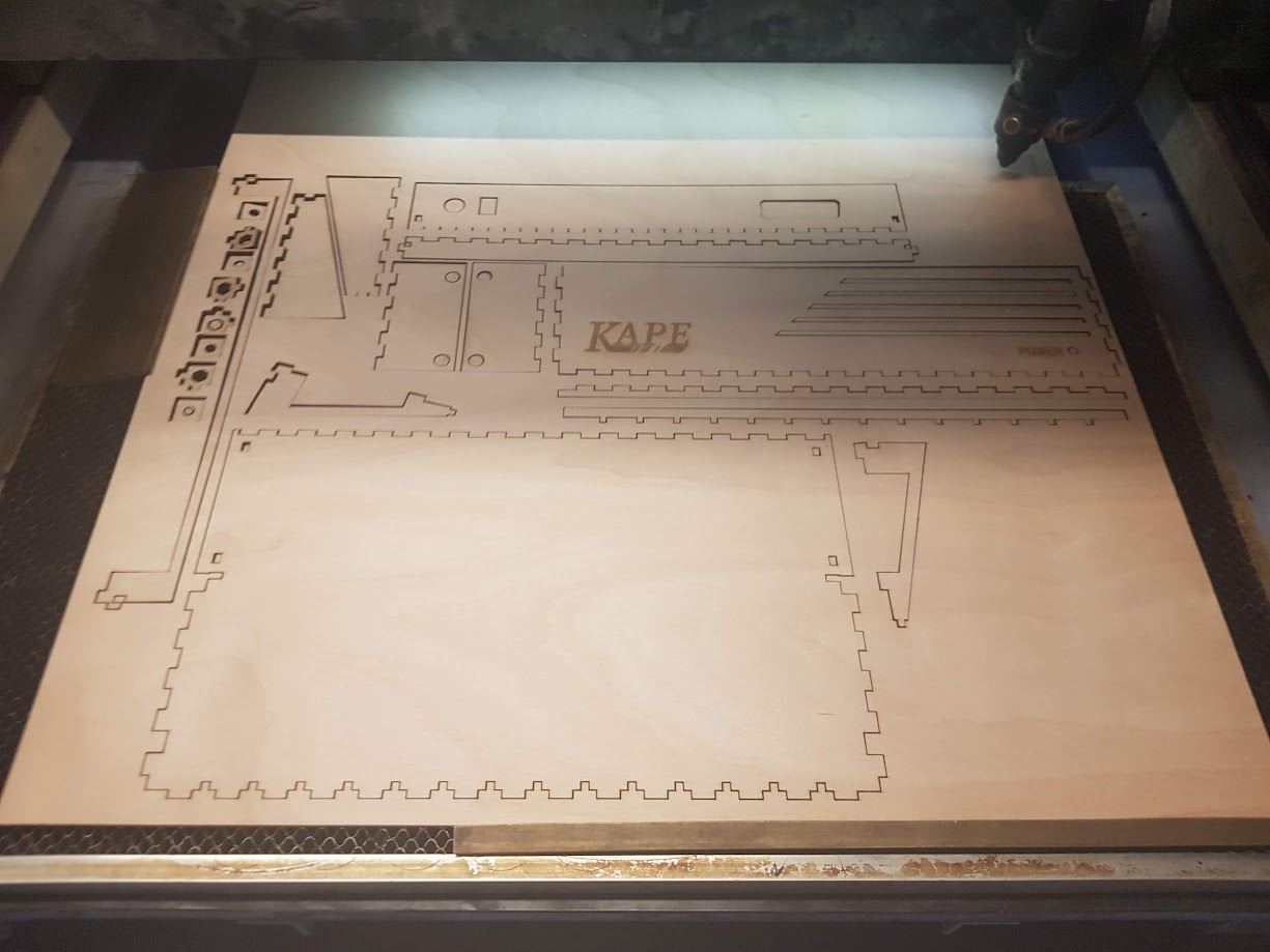
Currently I'm moving on from the GPU to the CPU side, and I've already setup some preliminary 6502 hardwired testing. Next up: PCB design for the GPU with KiCad, and 6502 CPU setup with 64K memory and 6551 serial and communicating between PC and the CPU!

maanantai 9. marraskuuta 2020

The Search For New Output

Well, this has been both frustrating and fun at the same time. As you might know, I lost my CRT to power issues (possibly a bad cap that just needs replacing). After that loss, I've been trying to come up with a way to present the output from KAPE GPU so that I could continue on the software portion while I wait for a replacement CRT or parts for the broken one. I came up with a few possibilities I could try out:

  1. Create a software emulator on the PC that I could work with to improve the GPU command structure
  2. I happened to have some MC1377P RGB to Composite encoder chips on hand - just wire these up and use my composite capture card to view the output on PC
  3. Modify the circuit a bit and do an additional grayscale weighted resistor DAC to be tacked on the sync line, which would work as a grayscale version of the screen and capture that
So, about option 1, software emulation - nah, don't feel like it. It would probably get Wreckless Abandon (the 2D platformer I'm doing on the side to be played on the end product) development forward as well, and I could possibly do it so I just had a similar framebuffer memory as in KAPE GPU, draw that every frame with say MonoGame, and do some interprocess communication method to send bytes to the simulator (instead of using the COM port to an debug interfacer UNO). If I cut enough corners, I'd probably even manage it in a few hours. But this project isn't about software, it's about hardware. So I want to do a hardware solution for this.

I (Don't) Got The Power!


So, 2 it is then. Oh boy did I have a lot of problems. And spoiler alert, in the end I didn't even manage to make it work properly. My first problem was power: the MC1377P (datasheet) actually needs +12V, not +5V. Luckily the chip has an internal +8.2V regulator, so the Vcc can be unregulated. But how do I get +12V from +5V? I had the idea of making a charge-pump with some capacitors and diodes and a PWM signal from an AVR chip (or the UNO), but either I screwed something up, or you just can't get enough current from a DIY charge-pump. (The chip needs 35mA on normal operation). 

I then found some ICL7660S (datasheet) negative voltage converter chips on my chips-pile, and reading through its datasheet, it could be wired as a voltage doubler, and it should just have enough current to make things going. I'm yet again on the territory of "either I have no idea what I'm doing" (to be fair, I actually don't!) or perhaps the chips were faulty/chinese fakes/etc. as I couldn't get them to work at all. In the end I tried just wire them up as their normal usage and do a negative voltage converter, but even without a load, I couldn't get -5V out where it was supposed to come out from, at no load.

I quickly realized I'm not going to be able generate +12V from +5V, at least with my current components or knowledge or both. So, I started looking for an alternative. I do have a +18VAC wall plug, and a useless (these days, it wasn't then) board that has a fitting barrel plug, so I was thinking I could maybe make a full bridge rectifier with some diodes and filter it out enough to be in the 10-14V range MC1377P expects power to be. However, I decided to try something else first. My second monitor's power brick's capacitors went kaput a while ago, and I ended up hacking up a power cord from inside my computer from the PSU that delivers 12V to the monitor. So, I luckily had one available Molex on the power cord, and an extra Molex cable to use as a donor to cut up, and I whipped up a 12V Molex to 2-pin header power cable to be used on the breadboard from a connector from the PC's PSU. 

After all this, I tested the chip with a volt meter on the power pins. I should get 12V and 8.2V (Vcc and Vb, the internally regulated output voltage). What I got: 8.4V and 7.2V. What's even weirder, if I tested the voltage between +12V and ground wrong way, I didn't get -8.4V - I got -24V instead. I was at a loss. I tested all the chips I had this way, and none worked. I was ready to throw the towel in (at least for now) but then I came by a simple MC1377P circuit design:


I noticed it had filtering/decoupling caps at the +12V line. I didn't have 47uF cap handy, so I substituted it with a 22uF one. And lo and behold, the voltages started to make sense again! In fact, using this schematic, I ended up finally taking some strides forward in this whole ordeal.

Wired almost according to the simpler schematic.
12V power not connected, nor the RGB lines.


It's Not Progressive Enough!


Now I finally had something nearly-almost working. However, when I tried to capture the image with my capture card, it couldn't sync to the image. I tried plugging the composite cable from the KAPE GPU to the capture cards component input Y channel as well (this should just read as a sync + luma), and it still didn't sync. I had an inkling it was because my sync generation generates a progressive 288p signal, instead of an interlaced 576i signal. However, as I had taken great care to implement the equalizing and serrated pulses properly, all I needed to take care of was to make sure there was the correct amount of frame end and frame start equalizing pulses on both even and odd fields. I might be mixing this around but I think even fields should have 5 pre-equalizing pulses and 4 post-equalizing pulses, odd fields 6 pre and 5 post.

The synchronizing pulses for VSYNC in an even field.

It seems to be a bit hard to find out information about PAL and NTSC signals in a concise and easy-to-digest format, but this page (http://martin.hinner.info/vga/pal.html) helped a lot on getting this right. Thanks Martin Hinner!

I finally got the capture card to sync, and to debug and make sure all other timings were correct, I also implemented option 3 - grayscaling the 4 bit color value with weighted resistors - for helping me debug the new interlaced sync. I had to do some fiddling with the framebuffer read timings though, before getting everything working properly. In the end this actually worked really well - I finally got a picture from KAPE GPU to my very, very picky capture card.


I even tested it out with our LCD TV.


Btw. the TV's composite in is a LOT less picky on the timings than the capture card. I could basically massage the values every which way, I even accidentally disable all the serration and equalizing pulses and it still worked, but the capture card didn't capture it the moment one value was off by one. However, even the TV couldn't capture the progressive output, which is a shame. And kinda also the reason I prefer to work with a CRT with this project, as they support 288p out of the box.

I Want Some Color In My Life


So, now we have the proper sync timings, and we also have power to the encoder chip. All we now need is color through composite with the help of a chip, and that should be to just connect the lines and be done with it, right? Well, not so fast. The chip needs a 4.43MHz crystal oscillator for the chroma subcarrier reference. I don't have that. I do, however, have a 17.73 MHz crystal, which is incidentally 4 times as fast. So I could use the 17.73 MHz crystal with the KAPE Pixel Timer AVR chip (ATtiny84) replacing its normally used 16 MHz chip and 4.43 MHz clock with a timer.

Luckily, I push the pixels out from the FrameBuffer FIFO with an AVR clock divided by 4, so I get this clock actually for free. Using the 17.73 MHz clock though would mean that the pixel clock would be almost 9 MHz instead of the earlier 8 MHz, but it should still work correctly in the end - the 256 pixels long line would just be a smidge shorter, and the individual pixels a little thinner. 

Theres another problem though - can the MC1377 be driven with only a clock on oscillator pins, or does it expect something else? With a little help from eevblog forum, I realized that MC1377 expects a color subcarrier wave reference, not just simply a timing reference, which would be a 0.5 - 1 Vpp sine wave if you are driving the color subcarrier externally. Now, I didn't find anywhere in the datasheet at what DC bias the chip expects this sine wave at (0V?), so I just did a voltage divider from 5V through a 330 ohm resistor and a 100 ohm to ground and filtered it once with a 1 nF cap to ground. The result should be something along these lines. 


So, now that I have managed to tackle the power issues, the interlaced syncing issues to get the image to my capture card, and the chroma subcarrier wave the chip expects, I should be all fine and dandy? Well, let's see, after I wired everything up (the earlier shown simple MC1377 circuit design helped a lot with this!), I wired the RGB lines through 22 uF capacitors and sync I connected straight up (the chip should be okay with a normally 5V signal that just has sync tips dropped to 0V), and connected the composite cable through a 75 ohm resistor to the capture card composite cable ANNNND....


Umm. Well. That's not what I expected nor wanted. With a quick glance, it seems every other line is skipped (and it actually changes every frame which lines are skipped), the colors are obviously out of whack, they shimmer a lot, there is a lot of noise etc... but I'm so close I can taste it!

However, I feel like I've sunken too much time on this already. I'd really want to figure out what I'm doing wrong, and how I could fix it, but it feels like the MC1377 is a lot more trouble than it's worth. Something like AD725 seems like a lot easier to deal with, and doesn't need a separate power supply if you are already using 5V. It also uses the 4Fsc crystals which I have (the 4 times the color subcarrier frequency, ie. 17.73). The biggest downside is it's a surface mount - I'm trying to avoid surface-mount chips as much as I can, though in case I won't find anything better, I'll gladly use one. I don't really like soldering in general, and the only soldering I enjoy is through-hole - at least right now, maybe with some practice I'll learn to enjoy soldering surface mount parts as well.

Fine, I'll Just Get A New One


Not long after my old CRT broke, I managed to source a replacement 14" PAL CRT with SCART. However, it was a bit of a drive away, and my back went a bit bad a few weeks ago, so I've been avoiding driving long distances to let it rest a bit. I was hoping I could get the colors working with the MC1377, but as I was nearing the realization that it's a lot more trouble than I want and my back has been feeling a bit better lately, I decided today was the day to finish the deal and get that replacement CRT. 


I'll finally be able to get back to actually implementing the GPU, instead of fighting with components I barely understand. The image is still in black and white, but tomorrow I'll move the CRT closer to my setup again, and hook up the CRT and we should have sweet, sweet RGB color again, in all its 4 bit RGBI glory that KAPE GPU outputs!

Now all that said... Having a composite out in addition to SCART would be a nice thing to have on the GPU (if not separately, then just populate the SCART Composite pin with proper Composite data)... Maybe I should get back to MC1377 (or some other RGB to composite encoder chip) at some point in the development cycle? But at least for now, I'll let it be, get the CRT setup again and I can get back from this detour and get back to defining the GPU commands and actually making sprites work!

Project update 2023

So, last post seems to be from summer 2021. Not even that long ago, eh? :D Well, time for an update then! Anyhoo, paradoxically a lot has ha...