So, last post seems to be from summer 2021. Not even that long ago, eh? :D Well, time for an update then!
Anyhoo, paradoxically a lot has happened regarding the project, and also, not so much. Summarizing:
- Laser-cut plywood prototype case
- KAPE GPU PCB version
- Address Decoder design
- Plan for the CPU board
- Plan for the keyboard
Laser-cut Plywood Prototype Case
Early this summer I had the possibility to use a laser cutter. I of course opted out to use it to print a new prototype case for KAPE. I now finally managed to assemble it! Pictures tell more than a thousand words, so have over 5000 words:
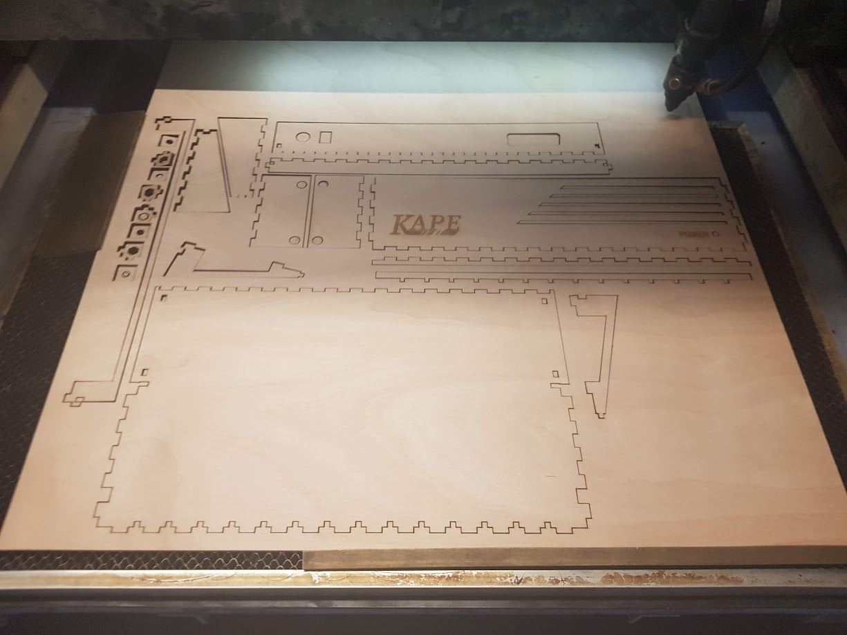


I was thinking of finishing the plywood with some wax oil - it might make the wood pop visually more, and also would give it a protective coating. I'd have to try the one I'm thinking of using on a scrap piece of that same plywood to make sure it looks good and doesn't ruin anything.
The backplate also doesn't have all the necessary outputs yet. There's only a reset button and a power switch, as well as a hole for SCART. The access to the laser cutter was very time-limited, so I had to rush the design a bit. If not for that forced rushing, I'd have designed a changeable backplate.
The top cover can be lifted, and is secured with screws on the side. I made them sunk by adding a plywood spacer in the holes. With more time I'd've thought of a better position for the screws, as it's quite annoying that the screws are on the side. But at least this way you don't have to flip the computer to get to the screws, or the screws being ugly and visible at the top.
Also, the current breadboard version, and possibly not even the minimized breadboard version, won't fit in the case, but the PCB version should fit nicely. I haven't even designed it yet so this is just wild guesswork.
KAPE GPU PCB Version
KAPE GPU has been transferred to a PCB version - however there were some bugs. I forgot one important resistor between +5V and SCART select source signal, so that the mode is changed from composite to RGB.

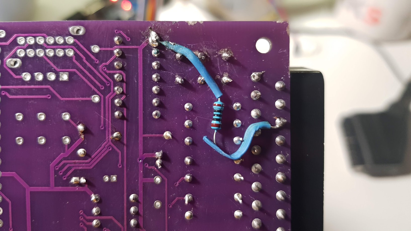
The board isn't fully populated yet - I soldered just enough parts to test that the AL422B I bought specifically for this board works properly... ...and it didn't. It ALMOST works - everything else works fine except D0 out. This could also mean D0 in could actually be the one that is broken. OR the chip's bit 0 circuit is fried.
I tried to bughunt in case it was something wrong with my routing or maybe I have a short somewhere or some other design blunder that makes it not work properly, so I tried stuff like cutting a specific ground line and jumpering from another side, etc. but it just looks like the chip is borked. Either I broke it, or it was broken when I got it.
I will be doing a thorough re-test, and if I can't figure it out, I'll try to desolder and replace the AL422B chip with another one I have on hand. If I'm not able to desolder it, I'll just populate a new board - I still have some spares left.
Address Decoder Design
I recently mulled about the Address Decoder. I have been thinking about external buses and peripheral cards and auto-config or manual config etc., but I decided I was thinking too complex, at least for now. So I revisited the Address Decoder, and it's still maybe a bit too complex, but it's a lot more simple than what I was thinking earlier.

I mean, sure, it looks a lot more complex than the one I presented in an earlier post, but that only had RAM, RAM and ROM, or RAM, ROM, and GPU in it. I talked about having a comparator for each device to select it, but that would result in one comparator per device PLUS all the needed glue logic. This way, I can get 8 devices with only 6 chips. With a PLD that count goes to 2, if you want to keep the device memory tightened to a single 256-byte page, or just the PLD if we forgo that and reserve 2K for device memory mapping.
This is the resulting memory map from this address decoder design. Oh and I have already started breadboarding it!


Plan for the CPU Board
Currently the CPU board (as of now, still in breadboards) looks like this:

I have circled red everything that will be (eventually) going the way of the dodo. In essence, my plan is to strip all debugging and uploading, remove the overtly complex clock design, and remove the old address decoder. I will be adding a ROM and at least the UM6551 for serial communication, a single clock source for 2 MHz, and the new address decoder. With any luck, it will only take 4-5 breadboards and fits in a lot smaller footprint. I might even be able to fit it in the new prototype case even if they were still on breadboards!
First tho, I will be fixing the current wirings, for helping with programming the ROM and UM6551, which I will be adding to it once I'm sure everything works correctly. I'll also probably get rid of the old address decoder and old clock at this point and replace them with the new ones. Once everything is working, I'll get rid of the debugging systems and minimalize the whole thing. At this point I'll hopefully have also figured out how to program an ATF22V10C (or GAL22V10) chip, so I can get rid of most of the address decoding chips.
After that, it's just adding the 6552, SD card interface and YM2149F, figure out the outputs and cabling and power, and we're as good as done!
Plan for the Keyboard
The keyboard has 61 keys, and the plan is to have the the keyboard controller send the scancode as a 6-bit value, and also as ASCII every other byte. Using 7-bit ASCII, we get the top-bit be an identifier bit in case the CPU side gets somehow out of sync. The unused bit in the scancode could then be used for state change info. The data is presented to the CPU only if there is an event, otherwise reading the keyboard controller results in a 0.
8bit keyboard read data
00000000               No event. Read again, if another zero,
                       no key events since last full read.

0ESSSSSS
||     |
||     \-- bits 0 - 5: SSSSSS - 6bit ScanCode
|\-------- bit 6:      E - 1bit Event, 0 -> key released, 1 -> key pressed.
                       If key pressed, next byte is and ASCII of this scancode
\--------- bit 7:      0 -> Scancode 1 -> ASCII

1AAAAAAA
|      |
|      \-- bits 0 - 6: AAAAAAA - 7bit ASCII
\--------- bit 7:      0 -> Scancode 1 -> ASCII
The keyboard matrix scan will be processed 1 kHz fullscan, with a 15x5 keyboard matrix. When a key is processed it's state is detected with the matrix scan, and compared to a previous state. In case the state has changed, the scan code is enqueued in a queue-buffer. If the state was pressed, the scan-code is translated to ASCII, bit 7 is set, and that also is enqueued.
I will use the ATmega16A for the keyboard controller, as it has more than enough pins to do a 15x5 matrix, and some control signals. It will be too slow to interact with the databus with interrupts, but with a little help from our friend, the 74HC573 tri-state latchable register, we can use the address decoders Keyboard Read -signal as the OE for the register, and also as an interrupt to let the Keyboard Controller know that a value has been read.
Even if the ATmega16A isn't fast enough to respond directly to a databus, it's more than fast enough to read a value from the queue buffer and output it to a register. If my calculations are correct, 6502 takes 4 cycles to LDA absolute address, and I will be running the 6502 at 2 MHz. That means the keyboard controller has 8 cycles per a 6502 cycle. If not with C, hacking with some assembly I'm sure I can make it work.
When in the interrupt, we'll dequeue the next scancode/ASCII from the queue-buffer, and latch it to the register chip. In case we don't have anything to dequeue, we'll latch 0. This lets the CPU know that now keyboard events have happened. Since reading the register is the only way to update it, the 6502 might need to read 0 twice to make sure we don't miss any keyboard input in a frame.

Summa summarum
So, been awhile.
Not much has happened, but there's definite progress anyway. Baby steps but steps anyway. Once I get (in the next 12 months, I bet) the GPU (both breadboard version and PCB version are currently "offline") fixed, the ROM installed, and the UM6551 serial connection for program upload done, I can start to figure out things like 6522, SD card interface, keyboard, YM2149F, gamepads/joysticks, etc.
Still haven't decided whether I'm gonna use NES pads, SNES pads or regular C64/Amiga -style joysticks, but there's plenty of time to figure it out.
Here's hoping I'll make the next blog update a bit earlier than in 30 months next time!


Ei kommentteja:
Lähetä kommentti