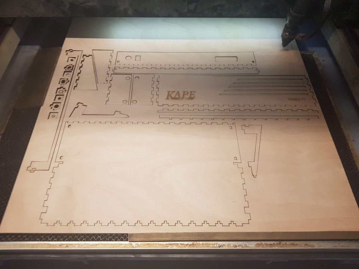
It's a been a hot few months since the last blog update. For my defense, nothing really major has happened with the project, even though I've been working on it with relatively the same speed and intensity as before. The biggest reason for this is that it's been mostly busywork with wiring up the mainboard. This is the latest iteration of the KAPE MB in all its glory (with annotations!)


However, my 2K EEPROM chips (AT28C16) still hadn't arrived, after waiting for months, and gradually having nothing else to do with the project, I decided that fine, I'll just wire up the memory and program it with an Arduino UNO to get some code in there. This, of course, added more complexity.
With this approach, I had basically 3 problems to solve now:
- Writing to the Data Bus from the UNO
- Writing to the Address Bus from the UNO
- Decoupling 6502 and keeping it inactive while UNO is accessing the Data and Address Buses
Tackling the board
The problem of writing to the data bus from the UNO I solved by using a 74HC595 Serial-In-Paralle-Out chip to be able to output 8 bits of data to the data bus with 3 pins on the UNO side. I was thinking of doing all 8 bits to as separate pins, but then I would have had to do some bit shifting for different output ports, and I wouldn't have had that much pins available for other control signals. Yes, I need to do a lot more bit shifting now, but at least it's straightforward and all towards the same pin. This takes a bit more cycles but uploading a 64K binary through the serial to the mainboard takes about 30s with current speeds, so it's fine.
In hindsight, I could've just used three 74HC595 SIPOs in series. I'm not sure whether it would've made it more complicated or more simple, but it would've been a possibility. The thing I like about the current way I wired it up is that it's a bit more compartmentalized. I can latch the hi and lo bytes of the address to the address registers, and I can manipulate the data in the data bus with the SIPO chip and don't have to worry about messing up the address bus at all, whereas with three SIPOs in series the address bus would get all messed up if I messed with the databus, and I'd had to write all 24 bytes in succession everytime. So perhaps this method was better after all. That said, this actually "only" helps with debugging and development, I still have to write all 24 bits everytime I write to a memory location when sending a full binary from the PC.
Now that I have writing to the buses setup, there's one more hairy problem remaining. The 6502 doesn't tristate the address bus at all. The data bus is tristated as long as reset is low, but the address bus is always driven when the 6502 has power. This is different in the new W65C02S chips from Western Digital, but when I was wiring this up the post hadn't delivered my order of one to me yet. So, I was stuck with a chip I didn't know what it actually was (it was a rebranded and painted over chip from aliexpress, I think it was labeled as R65C02, but cleaning it up with IPA it had markings of CMD G65SC02 chip, and I'm certain I saw even a third set of markings in an engraved form that was neither of those, so I have NO IDEA what chip this is, but... it seems to be a 6502 that I can run slowly, so I'm happy). As far as I know, with W65C02S you could just keep both RESET and BE lines low and both data and address buses would be tristated.
Anyhow. My initial instinct to decouple the address bus from 6502 was to insert 74HC573 transparent latches between the 6502 and the address bus. These are almost like the 74HC574 registers I used, with nearly identical layouts, except they don't latch with clock, but instead they have a Enable Latch signal, which, when high, makes the internal register follow inputs. Thus I could just wire it up to follow the 6502's address lines, and decide with the ~OE signal whether it is driving the actual address bus or not.
However, this didn't work. It should have. But it didn't. Everything seemed to be okay, but when I tried to decouple them from the address bus by driving ~OE high (to tristate their output buffers), instead of tristating it, both of the chips just drove them low. It took a while to debug this, as sometimes it seemed to work, and sometimes there lots of flicker on the address lines, etc. Bus contention. In fact, all the 74HC573 chips I have had this, I tested them all out: it worked exactly as in the datasheets, except when trying to tristate the output, in which case it drove the outputs low instead. Are these broken? Are they rebranded fake chips? I was trying to find out what chip this could be instead, but not one of the chips I found had the same layout as 74HC573 and instead of ~OE they'd have a MR or tristatable otherwise.
The solution then was to use 74HC574s here too. I don't like this though, as now I have to clock them to get the addresses in the latches, but at least they tristate properly, and if I use PHI2 as the clock, it should be okay. At least it's been working with lower speeds just fine.
Driving with signals
Alright, now that we have a mostly working system for uploading data to the SRAM and decoupling the 6502 from the address bus, we still have one more thing to tackle before we can actually upload and run code in it: after the upload, I need a way to get the control signals from 6502 to the SRAM.
From the UNO side this would be simple - just wire the same control signals on both sides to the same pins, and tristate when not using to drive it. However, the 6502 wants to drive everything all the time, so it would not be that good to deliberately drive the same line that the other can't tristate. Now, I could add YARC (yet another register chip), that I'd control the ~OE from the UNO side, and tristate all UNO control signals when needed, but I decided to go another route this time.
Using a 74HC157 4bit data selector (which, incidentally, is used in KAPE GPU as the pixel nibble chooser), I select with the UNO which side's control signals we are currently using. The outputs are wired to their respective pins: R/~W to SRAM ~W, PHI2 to SRAM CS. I use a third selector as a makeshift inverter for the S (select signal coming from UNO) to also get !S. That way I can use S as the ~OE for the UNO address registers (S low means we are using UNO) and !S for the 6502 address registers (S high means we are using 6502, thus !S is low when 6502 is selected).
Time to rumble!
Now that we have a way to upload code to the SRAM, and a way to transfer control of the buses to the 6502, we can actually start programming, uploading data to KAPE and actually run it! Using a simple test program that tests writes and jumps, I can debug if reads and writes work correctly by just analyzing the address bus leds.

If everything works correctly, the program should execute the far-jumping code, and jump to the label 'far'. This I can easily analyze visually by just checking that bit 15 and bit 12 address leds are lit for a few cycles as the NOPs churn along.
At the end of the file, I make it so that the size is exactly 65536 bytes long and that the reset vector is pointed to $200, which I have designated as the start address of code. Zero page is used for, well, zero page access, and $100 is used for stack, so $200 is the first available code area.
To make this into a binary-file I used vasm (as per the videos by Ben Eater, I highly recommend them for jumpstarting the hobby, and even if you are already an expert, the videos are highly entertaining to watch anyhow). After getting a 64K flat binary file, I uploaded it with some simple serial uploading code.


Awww but I wanna output something!
Uploading and running code is all fine and good, but it's not really exciting, now is it? Some kind of an output would always be preferred - in the simplest, it could easily be an output register and some LEDs. Something that you can programmatically enable and disable and set a value to, without being coupled to a bus or anything. I did in fact think about just setting up YARL (yet another row of LEDs) with YARC, but decided against it in the end. I just didn't feel like looking at more LEDs at this point, as I have so many signaling and bus debug LEDs already.
The other idea was to wire up an 1602 LCD module, and do some address decoding for it. Alas, the post hadn't arrived for this yet either. Of course though, why not just use the one output we are designing this mainboard for in the first place?
As we had moved when the year changed, KAPE GPU was still packed, but with a little of fiddling and fixing some minor mistakes, I made sure it worked again. So, I now have an output, but I need a way to write to that output.
KAPE GPU's CPU interface is a uni-directional FIFO chip, that the CPU can only write to. So, if I do some address decode logic, I can just get a proper write signal, when a specific address is hit, and that's all there is to it. Unfortunately though... I don't have any magnitude comparators at hand - I have ordered some, (not) surprisingly - so I have to use common logic gates I have available. I have a bunch of NAND gates, some AND gates, and some OR gates. I wanted to keep the part and gate count as small as possible, so the way I have the address decoding currently setup is that I use only the top two address bits, A15 and A14, to choose whether I need to activate the write signal for the KAPE GPU or not.
ORing A15, !A14, R/~W and PHI1 (inverted PHI2) I get a write signal that gets low only when we are on the second-to-top 16K chunk, R/~W is low, and PHI1 is low (which is the same as PHI2 being high, almost. There is a difference, but it doesn't matter in this use case). This basically means that whenever I write to that 16K chunk of memory, it all goes to the KAPE GPU.

This isn't a problem though - the SRAM access is not gated in anyway, so the SRAM part works correctly whether or not we are writing to the address that activates "Peripheral Write Signal" or not. Think of it as a listener, it doesn't affect the system in any other way. This makes it easy to test and debug stuff, though for certain, will not be the end design. Using as little as possible for the address lines, I managed to get away with a single inverter (which I setup with a BJT transistor) and 3 OR gates (that got taken care of with a single 74HC32).
What next?
Immediate next steps are to actually wire the KAPE GPU into the KAPE MB, and make sure it works. After that I could program some interesting non-interactive programming things, like prime numbers or fibonacci or some fractal calculations. Some of these might require a lot more speed, so I might be needing to setup a new clock module that I can change with a button (a la Ben Eater) with either manual clock, adjustable slow clock, or fixed MHz class clock.
I also now have all the parts necessary for the keyboard build with the proto-proto, so I could do and document that as well. I have to improve the current address decoding though before I can wire it up and actually use it in KAPE.
I have come quite far with the system, enough so that I'm gradually thinking about what the device/peripheral memory mapping will be and what signals I'd need for modular peripherals. One reason for modularity is that I have many different ideas for how to actually implement the GPU board, so I want the possibility to change the GPU design with some relative ease after V1 is done. The other is that I don't know what kind of devices I want to interface with, so I think it'd be better to make it as modular as possible.

Granted, the address decoding gets a bit more complicated than necessary, but I was thinking of using an ATF22V10 to do the address decoding, so it would only require one chip. But that's a topic for another post!
Thanks for reading and, as always, feedback and criticisms are always welcome! I have a tendency to get wrapped up in technical details, so if anyone wants some of the more technical areas opened up in a bit more detailed and easier to read and understand fashion, don't be afraid to tell me so, I'll try my best to be more concise and understandable!
Until next time!


Ei kommentteja:
Lähetä kommentti